

Main features
- Closed‑loop lithography – Real-time depth control, error <1 nm, creates accurate grayscale.
- In‑situ inspection – Captures structure images immediately after etching with the same probe, instant confirmation.
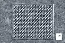
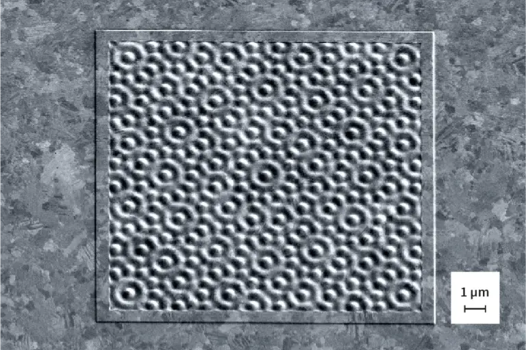
- Grayscale nanolithography – Creates 3D/2.5D structures for optics, quantum, cell frameworks.
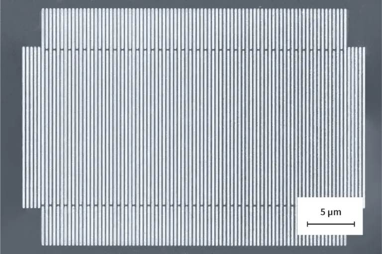
- Hybrid mix & match – Combines laser (DLS) wide area high-speed processing with t‑SPL for nano details.
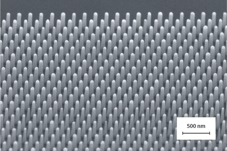
- Decapede module – 10 independent probes, increases throughput 10 times, resolution <50 nm.
- Markerless overlay & damage‑free – Precise alignment without markers, no damage to sensitive materials (2D, nanowire…).
Detailed description
Technology & principles
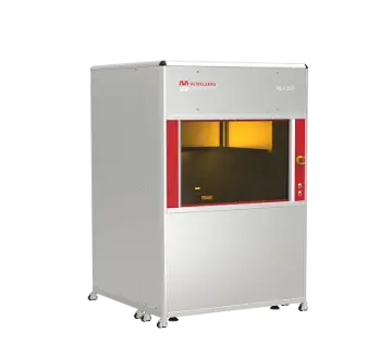
NanoFrazor uses a heated thermal probe to vaporize the optical barrier PPA, with no redeposition. It etches while capturing surface images (in-situ imaging), closed-loop control, ensuring depth accuracy to the nanometer. No proximity effect, no need for high vacuum.
Limitations of traditional lithography
- High-energy electron beams easily destroy 2D materials (MoS₂), nanowire.
- Creating 3D structures using e-beam requires many overlapping etching steps, difficult alignment, and large errors.
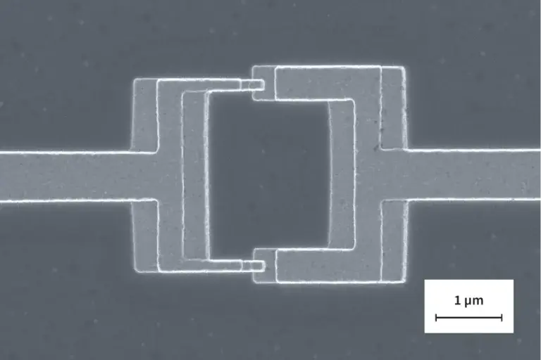
Advantages of the NanoFrazor maskless lithography system
- Damage‑free – uses heat, doing no harm to 2D materials, nanowire.
- In‑situ inspection – captures images immediately with a probe, no separate equipment needed.
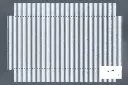
- Accurate grayscale <1nm – closed‑loop allows for the creation of cell membranes, gratings, waveguides in just one step.
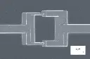
- Markerless overlay & auto‑stitching – alignment without the need for reference marks, ideal for single-layer transistors.
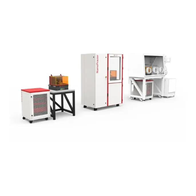
Integration & expansion
Hybrid DLS (wide area laser µm + t-SPL nano). Optional glovebox for air-sensitive samples. Standard transfer process (lift-off, etching, molding) with PPA + PMMA, PMMA/MA, PMGI.