
Key features
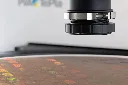
- Hyperspectral Technology: Combines spectroscopy and imaging to identify surface characteristics that are not visible to the naked eye.
- Non-destructive testing: Performs completely non-contact surface measurements, preserving the integrity of the product sample.
- Fast speed: Ability to capture and evaluate data in near real-time, optimized for production processes.
- Comprehensive analysis: Provides detailed information over 100% of the product surface area.
- Versatile: Replaces many individual measurement methods (FT-IR, SEM/TEM, LIBS, X-ray, etc.), saving costs and time.
- High accuracy: Measures layer thickness from 1 nm to 500 µm and accurately identifies types of contamination and surface defects.
- High compatibility: Meets ISO class 3 cleanroom standards, suitable for integration into modern production lines.
Detailed description
Technology & Operating Principles
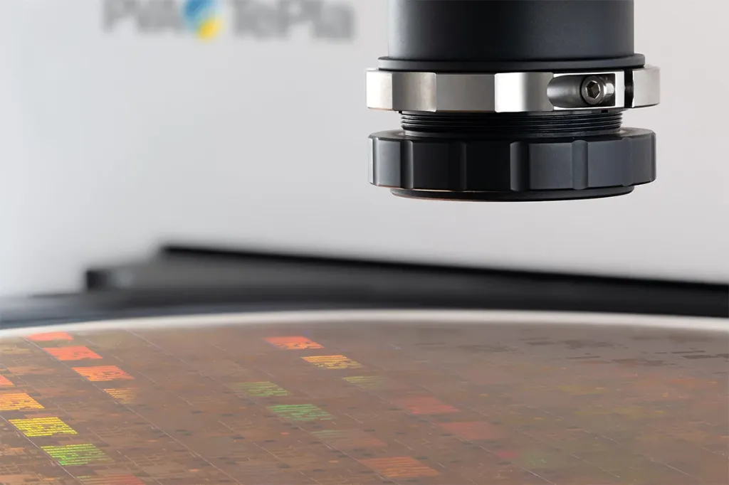
VEreveal® uses advanced Hyperspectral Vision technology to analyze surfaces. By combining high-resolution images with optical spectral data, the system can identify the chemical, electrical, and optical properties of the product surface. The specialized AI software VEsolve® PRO automatically processes this data to provide analytical results on surface status, film thickness, and deviations visually.
Solve the problem
In semiconductor manufacturing, contamination errors, film thickness deviations, or small surface defects are often difficult to detect using conventional methods, leading to a high scrap rate. VEreveal® addresses this issue by quickly scanning the entire surface (100%), replacing a multitude of costly and slow analytical methods such as SEM, AFM, or contact angle measurement, thereby helping to ensure strict quality control and optimize the process.
Integration & expansion
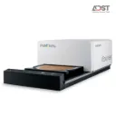
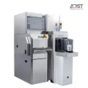
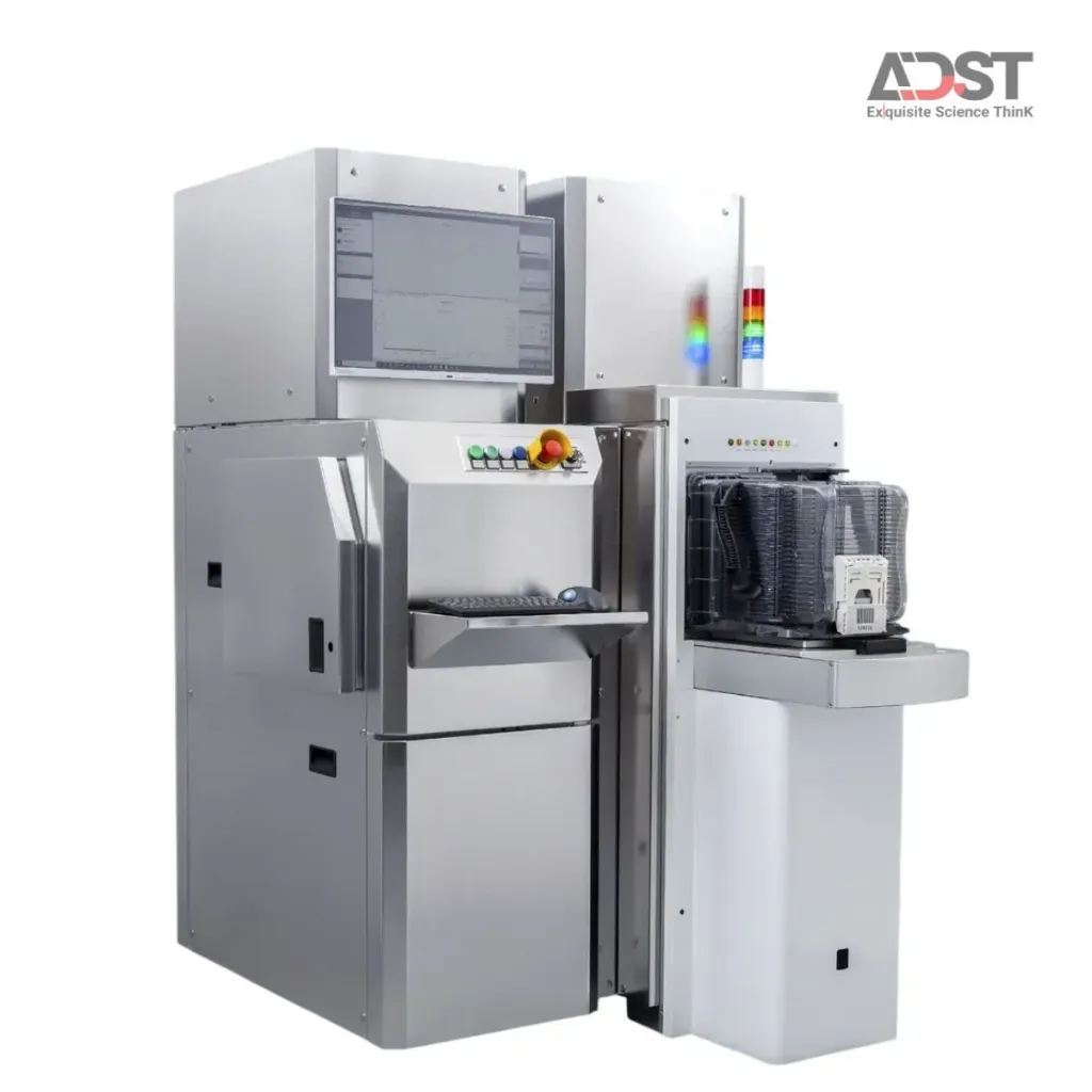
The device supports wafer sizes up to 300 mm and has flexible configurations: MACRO for macro inspection, MICRO for micro inspection, and FUSION for both. With a design that meets ISO class 3 standards and flexible connectivity options, the system can easily be integrated into stringent production environments for automated control.