

![youtube - [Video]](/web/image/product.image/545/image_128/youtube%20-%20%5BVideo%5D?unique=f904523)
Key Features
Unique Versatile Platform: Allows the combination of thermal batch ALD modules and single-wafer PEALD modules on the same cluster system without breaking the continuous vacuum environment.
High Productivity: Equipped with a proprietary pre-heating module that eliminates waiting time, significantly boosting production speed.
Lab to Fab Scalability: Maintains the core hardware architecture from R&D machines (Transform® Lite) to high-volume production lines, minimizing risks when scaling up.
Fab-Ready By Design: Integrates a standard industrial horizontal wafer loading automation system, compatible with SECS/GEM communication protocols and certified for SEMI S2/S8 safety.
High Film Uniformity: Achieves extremely low film thickness non-uniformity of less than < 1% (1σ) across the entire wafer batch (WiW, WtW, BtB) for standard oxide films.
High Serviceability: The design optimizes access space, allowing engineers to easily perform quick routine maintenance, minimizing machine downtime (MTTCR extremely short).
Detailed description
Technology & Operating Principles
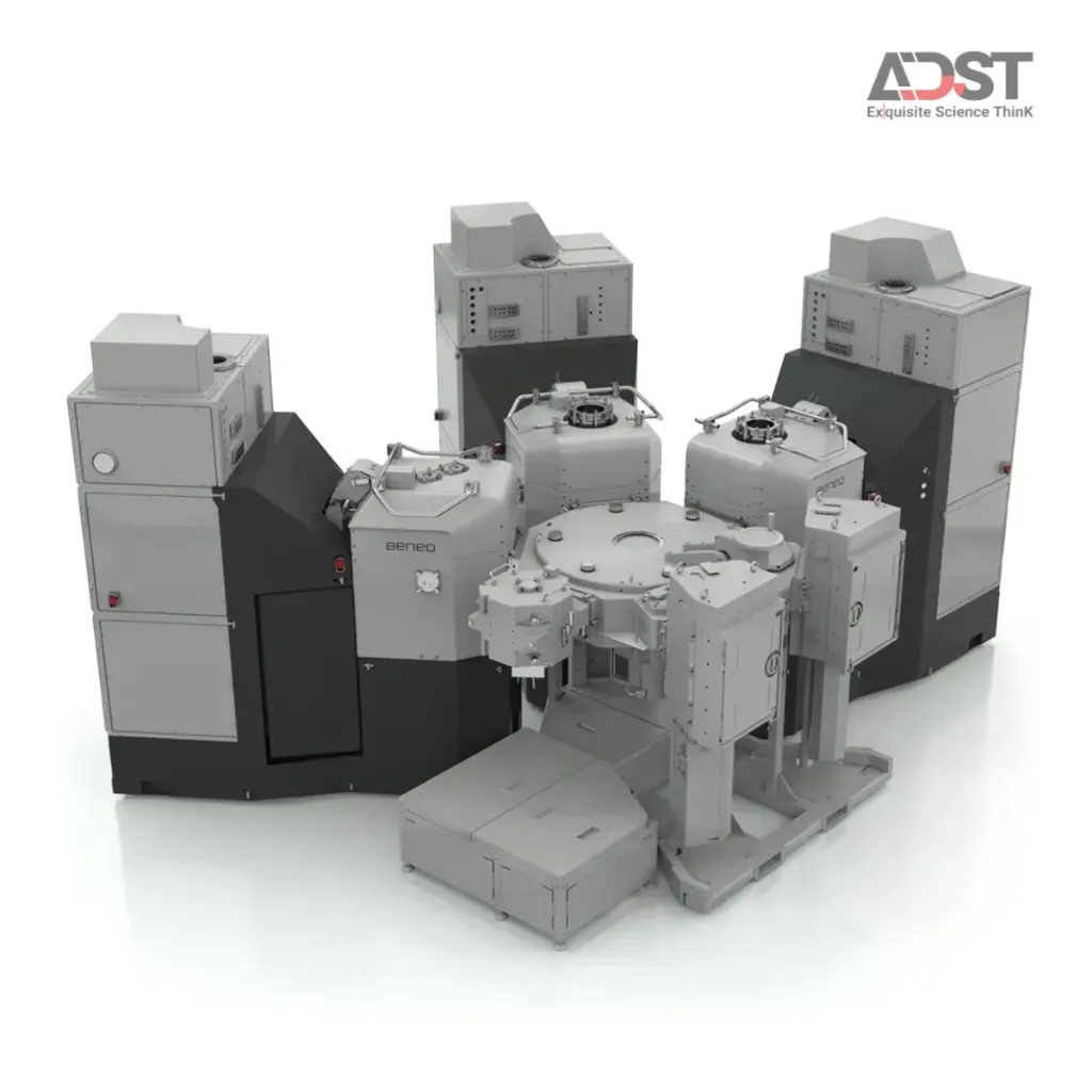
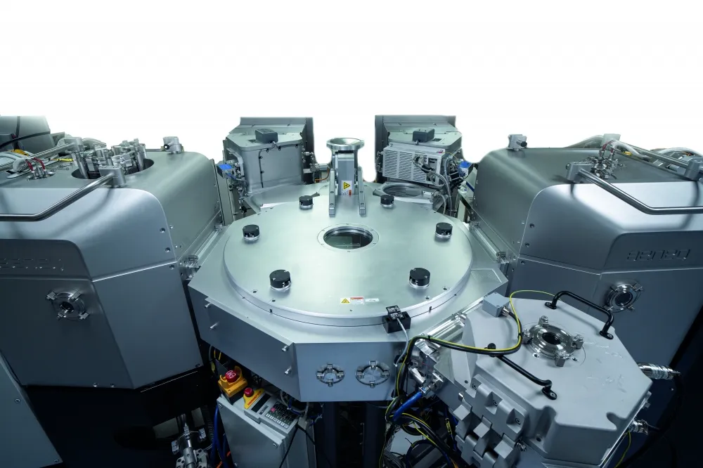
Beneq Transform® operates automatically based on a central robot cluster structure distributing semiconductor wafers to a maximum of 3 processing modules combined with 1 preheating module. The system performs a continuous 3-step exclusive film deposition/lamination process under high vacuum: Surface cleaning with plasma, interface transition layer deposition using PEALD, and protective dielectric film coating with thermal ALD. This flexibility allows for the deposition of an ultra-wide range of materials including oxide films, nitride films, and complex nanolaminates (Al₂O₃, SiO₂, HfO₂, Ta₂O₅, TiO₂, TiN, AlN, SiNₓ, ZnO, ZrO).
In More-than-Moore semiconductor manufacturing (especially for wide bandgap semiconductor components like GaN and SiC), controlling the quality of the thin film interface surface without contamination or oxidation between steps is a critical issue, while traditional ALD systems often have too slow speeds (long cycle times) causing the cost per wafer (CoO) to rise significantly. Beneq Transform® thoroughly addresses this barrier by maintaining absolute vacuum throughout the plasma-to-thermal cycle. At the same time, the "Mini-batch thermal ALD" technology (small batch deposition of up to 25 wafers) combined with the preheating cluster helps increase throughput from 15 wafers/hour (1 module) to over 40 wafers/hour (3 modules), reducing operational costs to an optimal level for the factory.
Integration & expansion
The system has the capability to flexibly resize wafers from 3", 4", 6" to 8" on-site and can be easily upgraded to the Transform® 300 configuration for processing 12" (300 mm) wafers. The equipment allows for flexible expansion through the addition of retrofit modules, integration of an automatic wafer handling system (EFEM), and configuration of additional liquid precursor lines (up to 3+1 lines) or special gas lines such as Ozone and Ammonia to broaden the high-tech application portfolio.