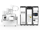

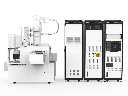
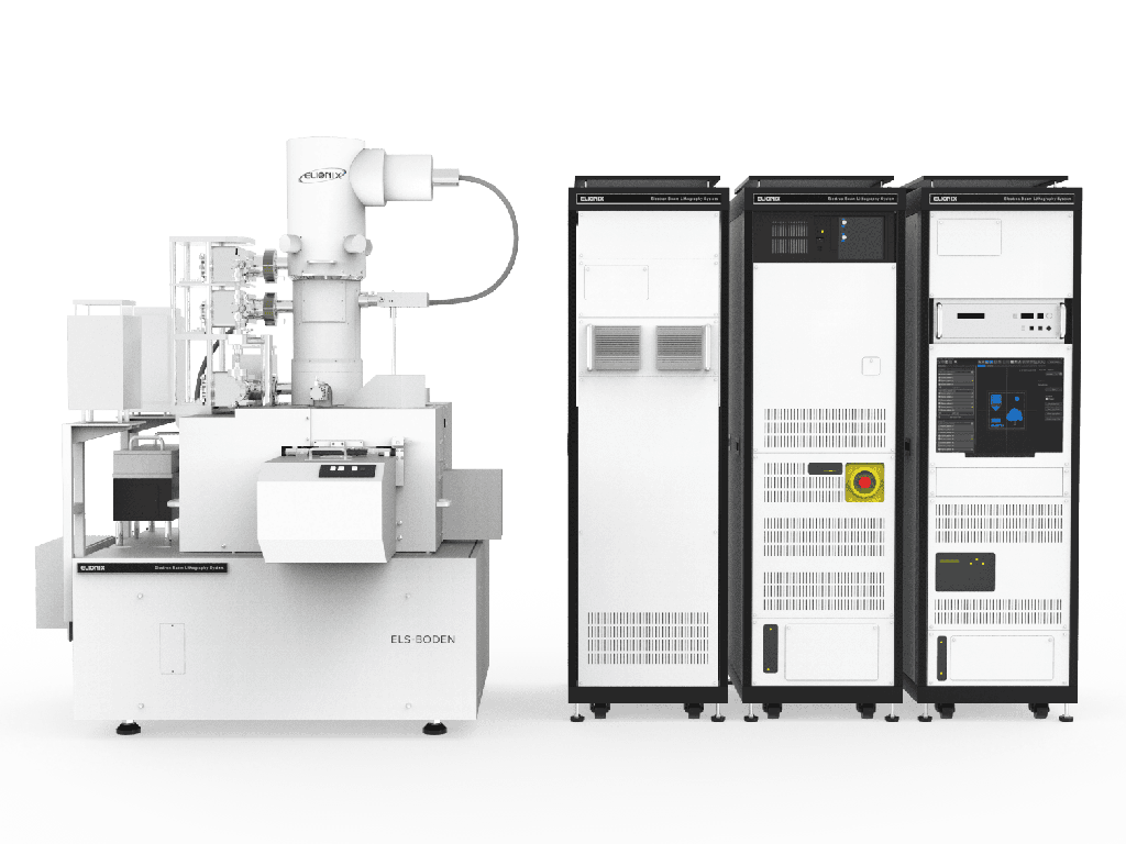
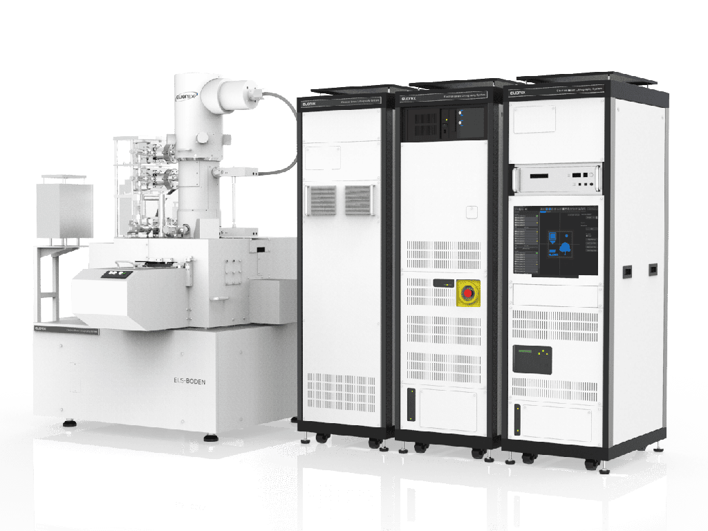

Main features
- Perfectly meets all stringent requirements (High Performance): Flexible voltage range options from 50kV, 100kV, 125kV to 150kV allow for optimal processing from high-speed production to ultra-fine patterns.
- Largest industrial-scale writing area (300mm Square Area): It is the first system on the market to comprehensively expand the exposure area to 300mm x 300mm, significantly enhancing throughput.
- Diversifying flexible sample sizes (Versatile Holders): Supports processing from small sample pieces in basic research to large 200mm/300mm Wafer sizes and standard optical masks (6025, 9025).
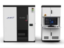
- Comprehensive operational automation (Automatic Loading System): Provides a range of hierarchical options from Single Autoloader for R&D rooms to Multi Autoloader and Robot loader systems (300mm FOUP / PEB) for automated production lines.
- Nano-precision beam positioning (Ultra-precise Positioning): Beam displacement resolution reaches an extremely small 0.1nm at the standard writing field, ensuring structural uniformity.
- Professional intuitive management and programming (Intelligent Software): The elms software integrates secure account management tools, intelligent exposure settings, and supports feature expansion through Python Scripting.
Detail Description
- Technology / Principles: ELS-BODEN fully inherits the core legacy technology of Elionix combined with the ZrO/W Thermal Field Emitter. The ultra-fine electron beam control system achieves a minimum beam spot size ranging from 1.5nm to 2.8nm depending on the voltage configuration. The new generation exposure scan clock achieves a maximum frequency of up to 200MHz, operating synchronously on the comprehensive elms lithography system management software platform.
- Solution: Research facilities and semiconductor manufacturing units often face significant bottlenecks when choosing between a high-resolution ultra-small structure system with low throughput or a large write area system with poor accuracy. ELS-BODEN completely eliminates this limitation thanks to its ability to combine ultra-high acceleration voltages of up to 150kV and the only full 300mm square exposure area on the market. The bottleneck of time-consuming manual switching between sample types is also thoroughly addressed by the automated loading system using robots customizable from laboratory to factory scale.
- Integration / Expansion: The device is designed with a very high modular structure with optional vacuum chambers of 200mm or 300mm. The sample loading system can be flexibly upgraded from a Single Autoloader to a Multi Autoloader system, specialized Robot loader for 300mm FOUP boxes, or a Robot PEB (Post Exposure Bake) system, allowing direct integration into mid-scale automated semiconductor production lines.