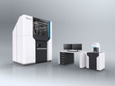

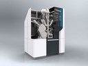


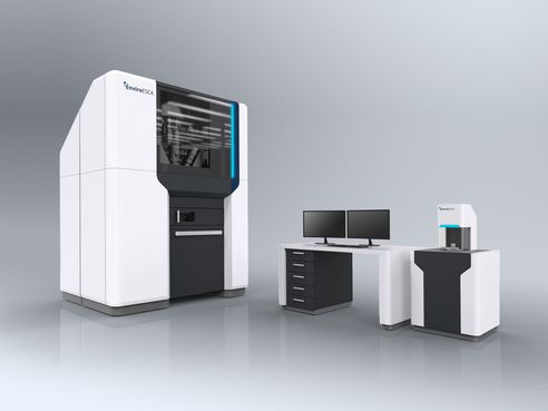

Main features
- Fully Automated XPS Metrology (Fully automated XPS measurement): The system automates the entire process from sample transfer, pressure control, setting measurement parameters to data analysis.
- Depth Profiling by ARXPS (Non-destructive depth profiling): Uses the ARXPS technique combining three variable X-ray energy sources (AlKα, AgLα, Cr Kα) to accurately construct the depth structure of thin films.
- True Hybrid Metrology (Multi-method hybrid measurement at the same point): Simultaneously integrates techniques for analyzing electronic, chemical, and optical structures such as SEM/SAM, LEISS, UPS/IPES, REELS, Raman, and IRRAS.
- Variable Atmospheric Conditions (Flexible operating environment): The ability to switch measurement environments flexibly from ultra-high vacuum (<5x10⁻¹⁰) up to the near-atmospheric pressure (NAP) mode up to 50mbar.
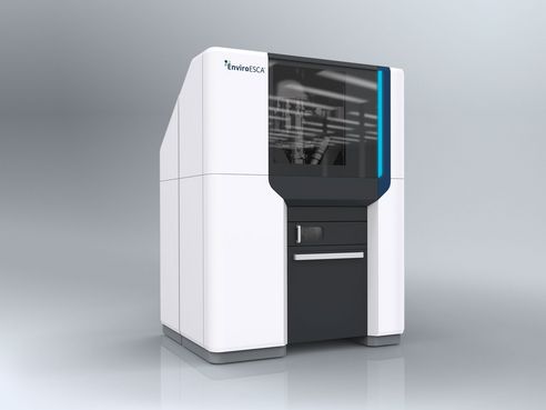
- Two Specialized Versions (Two versions to accommodate all sample sizes): Providing version configuration LAB (sample size up to 80x80mm for research and version FAB (supporting 8" or 12" full wafers) strictly adhering to SEMI cleanroom standards.
Detailed description
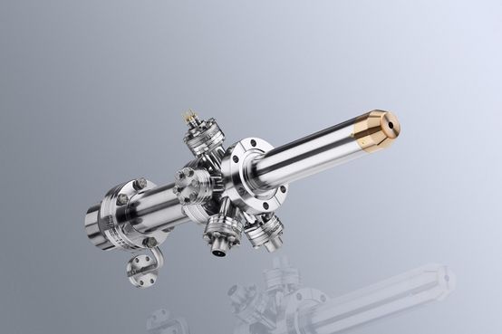
- Technology/Principle: EnviroMETROS operates based on the photoelectric effect principle developed from the traditional ESCA foundation. By stimulating the sample surface with monochromatic X-ray sources of different energies and collecting photoelectrons through a 150mm wide-angle hemispherical energy analyzer, the system allows for accurate quantification of chemical composition and bonding state with a detection limit < 1%. The unique point of the system is the application of Environmental Charge Compensation technology in NAP mode, enabling perfect analysis of polymer samples, biological materials, or insulators without the need for surface treatment.
- Highlights: In the semiconductor and thin film materials industry, analyzing the structure of deep layers often requires ion sputtering techniques (sputter profiling) that destroy the sample and risk altering its chemical nature due to heat. EnviroMETROS thoroughly addresses this issue thanks to its proprietary simulation software ITFAP combining multi-energy ARXPS data to construct non-destructive depth profile. Additionally, for semiconductor analysis, the need to cut the wafers into small coupon pieces to fit into traditional UHV vacuum chambers will damage the entire wafer and cause contamination. Version EnviroMETROS FAB with an automatic transfer robot allowing the entire 8" or 12" wafer to be placed into the analysis chamber, enabling the wafer to return to the production line after measurement.
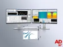
- Integration/Expansion: The system features a central control software Keystone M that comes with two advanced processing packages: ISQAR (Automatic peak identification and quantitative curve fitting) and ITFAP (Constructing thin film structures from angle-resolved data). For the LAB version, the system includes a flexible UHV connection port that allows direct linking to thin film processing chambers, the RapidLab C sample holder system, or gloveboxes to protect samples absolutely from the atmospheric environment. For the FAB version, the system communicates perfectly with automatic wafer loading robot systems through the factory's SEMI reporting software standard.