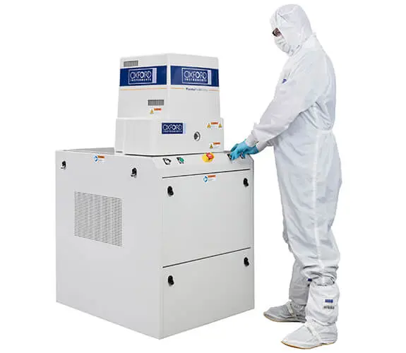

Key features
Diverse plasma technologies on a platform – RIE, ICP (Cobra®), ICP CVD, PECVD, combined RIE/PE, meeting all etching and thin film deposition needs.
Wide substrate temperature range – from -150°C (cryo) to +1200°C, with options for liquid-cooled electrodes, resistive heating, or cryogenic.
Proprietary ICP Cobra® source – high plasma density at low pressure, independently controlled DC bias, reducing wafer damage through electrostatic shielding.
PECVD with precise stress control – dual frequency showerhead (LF/HF), allowing adjustment of films from tensile to compressive or low stress.
Smart endpoint detection – laser interferometry (depth measurement), OES (by-product monitoring), optimizing yield and reducing maintenance costs.
PC4000/PC4500 software and clustering capability – intuitive interface, data logging (50ms), user permissions, SECS/GEM compatibility, up to 4 processing modules can be combined.
Detailed description
Technology & principles
The PlasmaPro series uses a symmetrical axial centrifugal pump chamber configuration with a direct short turbo pump, ensuring high pumping speed and low base pressure. The ICP Cobra® source generates high-density plasma at low pressure, with RF bias independently controlling ion energy. PECVD uses an RF-powered showerhead, mixing LF/HF frequencies to adjust film stress.
Common limitations of PECVD
- Laboratories need to process a variety of materials (Si, III-V, dielectrics, metals) with different processes (deep etching, low-temperature deposition, high-selectivity etching) on the same platform.
- Deep Si etching requires very low temperatures (cryo) or the Bosch process, while passivation film deposition requires low temperatures to protect thermally sensitive layers.
- Frequent chamber cleaning causes interruptions, chamber erosion, and increased costs.
- Failure analysis (FA) on packaged chips requires fast layer removal rates without damaging the chip.
Advantages of the PlasmaPro system
- Modular system: RIE, ICP, ICP CVD, PECVD can operate independently or cluster together, sharing a wafer loader.
- Cryo electrode (-150°C) and cryo-etch process for Si deep etch; ICP CVD deposits at temperatures as low as 5°C.
- End-point detection for cleaning using OES: accurately determines the end point, reduces chamber erosion, decreases particle generation, and increases yield.
- PlasmaPro FA with Plasma Accelerator (etching speed 20 times faster), processing from packaged chips to 200mm wafers.
Integration & expansion
- Cluster platform with a central transfer chamber (hexagonal or square), wafers maintained in a vacuum environment while moving between modules.
- Integrated laser interferometry (measuring etch depth, endpoint on small samples), OES (full surface/batch, chamber condition monitoring).
- Gas pod with a maximum of 12 gas lines, remote, safe, vented.