

Key features
Submicronic post-weld accuracy (± 0.3 µm): Ensures maximum yield on the most advanced microchip products.
Perfect parallel flatness alignment (< 1 µrad): Automatic mechanism adjusts the parallelism between two components before each welding cycle, completely eliminating axial misalignment errors.
Handling large-sized components: Supports chip sizes up to 100x100 mm on wafer substrates with diameters up to 300 mm.
Proprietary optical vision system: Provides ultra-high resolution alignment capabilities, combined with optimal welding parameter control.
Flexible transition from R&D to Pilot line: An open design platform allows for rapid configuration, perfectly accommodating the technology flow from the lab to small-scale production.
Nano structure imprinting capability (NIL configuration): Support for upgrading the Nanoimprint Lithography feature (using both Hot Embossing and UV-NIL methods) without losing the core chip bonding capability.
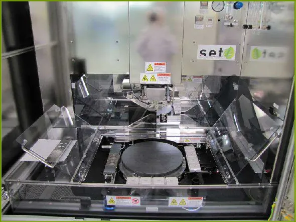
Protective gas welding environment (Confining gas): Integration of a protective gas processing chamber, including Formic acid, helps minimize oxidation of the weld.
Detailed description
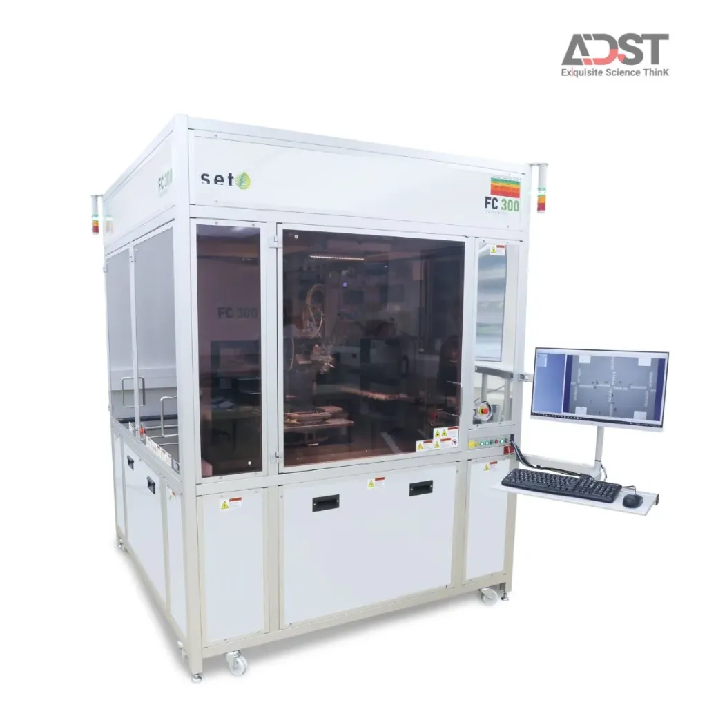
Technology & Operating principle:
The FC300 operates automatically based on a granite structure and air bearing construction, providing long-term stability. The machine works by aligning high-resolution optics combined with a High Resolution Motorized Pitch & Roll system to adjust the absolute parallelism to under 1 µradian between the chip and the wafer before bonding. The system supports a variety of bonding techniques: Thermocompression, Reflow (in-situ / mass reflow), Ultrasonic, UV-curing, and Adhesive bonding for fine pitch structures < 10 µm.
In high-density microchip packaging (such as 3D Integration or Cu-Cu bonding), simultaneously controlling extremely high pressing force (High force) and sub-micron accuracy without breaking thin/brittle components (fragile dies like GaAs, HgCdTe) is a significant challenge. The FC300 thoroughly addresses this barrier by allowing quick process head reconfiguration to smoothly switch between a very low force range (Low force from 1 N) for sensitive optoelectronic components, to an ultra-high force range (High force up to 4000 N) while evenly and accurately controlling temperatures up to 450°C.
Integration/expansion:
The device has the capability to process chips (Upper component) from 0.2 mm to 100 mm and substrate wafers (Lower component) up to 300 mm. The FC300 has strong scalability through optional modules (Options): Ultrasonic head, nano imprint lithography NIL system (Hot Embossing / UV-NIL resolution < 50 nm), vacuum/gas bonding chamber with Formic acid, and an automatic robot feeding system (FC300R) to optimize the production cycle.