

Key Features
- Ultra-small microscopic spot sizes: Supports a variety of measurement spot sizes (125µm to 5µm) through objective lenses (2x-50x), allowing for precise analysis of microstructures such as individual pixels on flat screens or the surface of wafers.
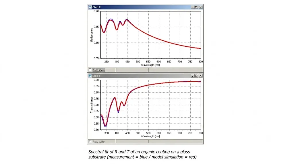
- Comprehensive multi-parameter analysis: Provides detailed measurement data on reflectance, transmittance across the spectrum, color coordinates (Color-R, Color-T), thin film thickness (both single and multi-layer) along with optical constants (n&k).
- Chromatic correction optical system: The objectives are specially chromatically corrected for an extremely wide spectral range from 380nm – 1070nm, ensuring optical stability and maximum accuracy under all conditions.
- Flexible integration (High Modularity): Easily connect the spectroscopic system and light source through a fiber optic system, with options for manual or motorized objective stage configuration to suit diverse research needs.
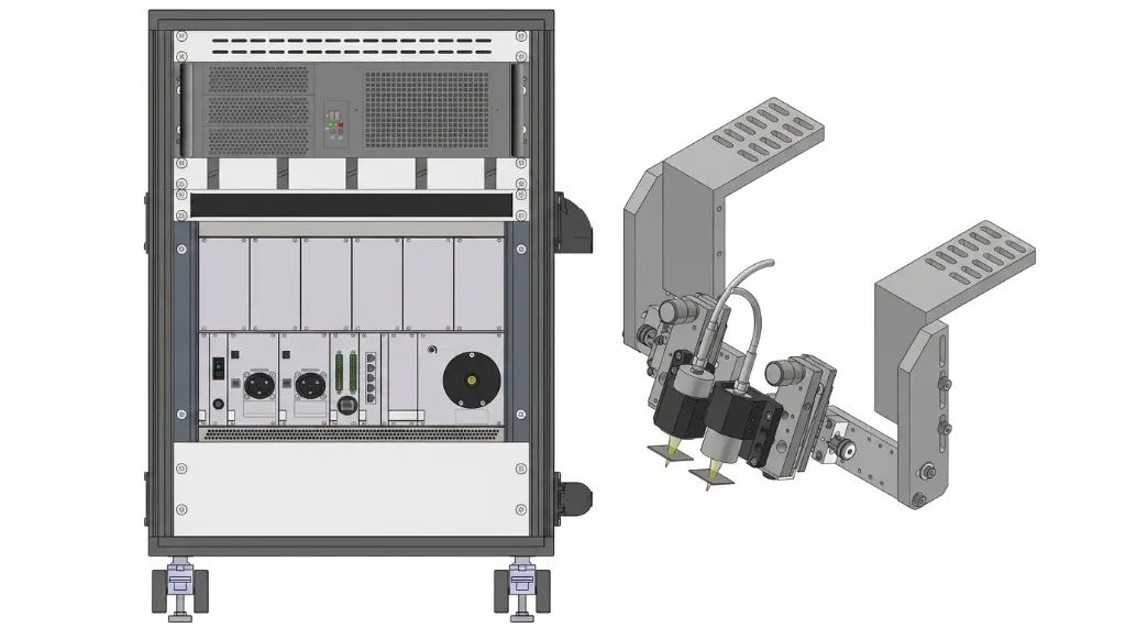
- Extended sample measurement stage (XYZ-stage): Offers options for manual sample movement (LITE version) or fully automated (SCAN version) with a movement range of up to 600x600mm, along with autofocus and pattern matching functions.
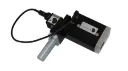
- User interface and camera: Built-in 640x480 CCD camera (USB interface) for observing and accurately determining the measurement location of the micro area directly on the software control interface
Detailed description
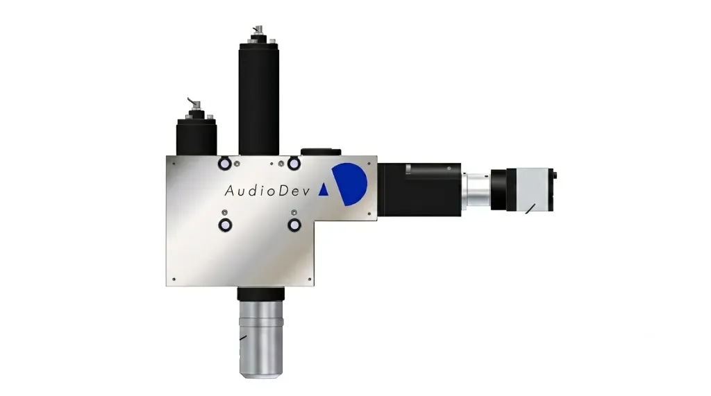
Advanced microscopy combined spectroscopy technology
The TCM µScope device operates based on the principle of spectroscopy (Reflectance & Transmittance) at a standard incident angle of 0°, combined with a high-quality microscope head. The system is equipped with a 50W Halogen light source (lifespan >2000 hours) and a VIS/NIR spectrometer (Silicon/InGaAs diode), providing ultra-fast sampling speed (< 200ms) with an R&T error of only ±0.4% [4]. The feature of coupling through a dedicated optical fiber system helps maintain the absolute integrity of the signal from the micro sample to the sensor.
Overcoming measurement barriers of micro-structured thin films
In semiconductor manufacturing or display components (OLED, TFT-LCD), controlling the thickness of non-uniform coatings at the micron level often exceeds the limits of traditional spectrometers. The TCM µScope system overcomes this bottleneck by narrowing the measurement spot size down to 5µm, ideal for measuring within each individual RGB pixel, MVA structure, ITO layer, or photoresist film. The system boasts an impressive measurement range, combining ultra-thin film analysis (2nm - 3000nm) using the Fit-method and thick film measurement (1µm - 25µm) using FFT spectral analysis algorithms with high repeatability.
Diverse integrated and expandable configurations
NXT provides flexible configuration solutions for all industrial challenges: The TCM µScope-LITE model is suitable for measuring the thickness of static materials such as packaging, coating of cans (CAN); while the TCM µScope-SCAN model equipped with an automatic XY table is the perfect choice for semiconductor wafer systems or large display glass (up to 600x600mm). The device also allows for the flexible option to add a transmittance measurement channel to fully capture the optical constant characteristics (n&k) for inkjet, vacuum coating, or photolithography technologies.