

Key features
- Wafer testing at cryogenic temperatures (< 2 K), allowing characterization of devices under the actual operating conditions of quantum chips and superconducting circuits.
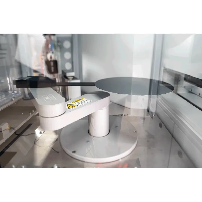
- Supports wafer-level characterization, enabling simultaneous evaluation of multiple devices on the same wafer, increasing R&D efficiency.
- Optimized for quantum computing research, especially in testing superconducting qubits, resonators, and quantum circuits.
- High-precision probe system, ensuring stable electrical contact in ultra-low temperature environments.
- Advanced electrical – RF measurement capabilities, suitable for high-frequency measurements and quantum signals.
- Integrated cryogenic platform design, reducing vibration and thermal noise, ensuring measurement accuracy.
- Supports automated testing, enhancing throughput for quantum industry research and development.
- Compatible with various types of wafers and measurement devices, flexible in experimental configuration.
Detailed description
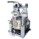
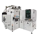
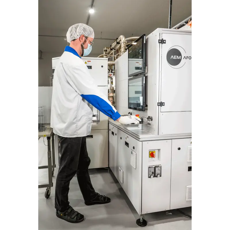
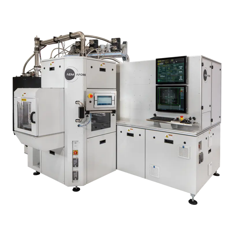
- Cryogenic Wafer Prober is a wafer testing system at cryogenic temperatures (below 2 K), designed for the research and development of quantum chips and superconducting devices. The system allows for the characterization of devices at the wafer level under the actual operating conditions of quantum circuits.
- Designed for highly precise electrical and RF characterization, the system facilitates the evaluation of superconducting qubits, resonators, and advanced quantum architectures. By enabling wafer-level testing, it maximizes measurement throughput and shortens the device development timeline.
- Leveraging a highly stable cryogenic platform, the system guarantees superior measurement precision while minimizing thermal noise. It seamlessly integrates with state-of-the-art measurement instruments, including VNAs, RF sources, and DAQ systems.