
Key Features
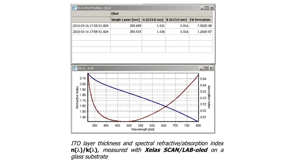
- Comprehensive multilayer measurement: Accurately determines film thickness (2–500nm), material spectra n(λ)/k(λ), surface roughness, and refractive index profiling for transparent conductive films (ITO).
- Non-destructive analysis: Non-contact optical measurement operations help preserve the original properties of the sample, suitable for transitioning between R&D environments and production control (QC) processes.
- High material compatibility: Testing and evaluating the effectiveness of most related coatings such as organic material films, dielectric films, to metal or conductive layers.
- Flexible 3D scanning map (SCAN): The Xelas SCAN-oled version supports x-y scanning (mapping), allowing for rapid multi-point spectral collection to assess the uniformity of thin films over a wide area.
- In-depth optical modeling: Proprietary oscillatory model algorithm allows for self-setting of material configurations (Optical Modelling), easily anticipating new materials and layered structures.
Detailed description
Advanced optical interference principles
The Xelas-oled device operates based on the analysis of the phenomenon of light interference generated by the phase shift between the reflected rays on the front and back surfaces of the film layer. Combined with measuring the light absorption capability that changes the wave amplitude in each layer, the system uses a proprietary oscillation algorithm to solve complex optical calculations. From there, Xelas-oled is capable of identifying ultra-thin film layers from 2nm as well as detecting even the smallest changes in multi-layered stack structures.
Addressing the quality barriers in OLED production
In the organic light-emitting diode (OLED) manufacturing industry, the quality of components is directly affected by the uniformity of thickness and the roughness of the coating material. Instead of costly destructive testing, Xelas-oled overcomes this barrier with extremely accurate offline measurements. The system allows manufacturers to timely detect the drift of local parameters, thereby maintaining stable production conditions and increasing the yield of finished components.
Flexible upgrades and expansions
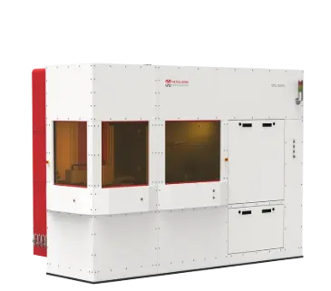
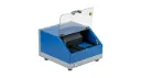
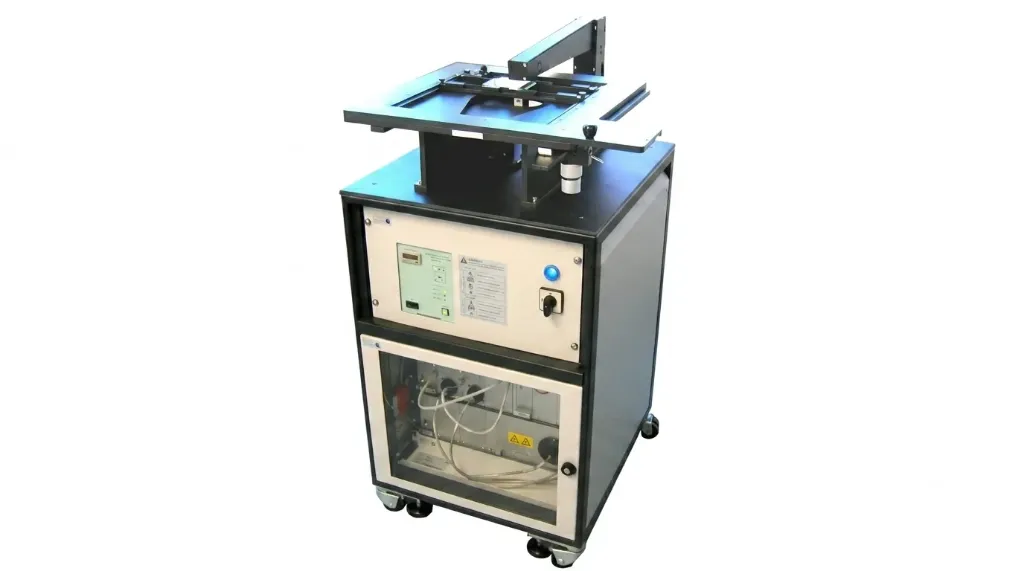
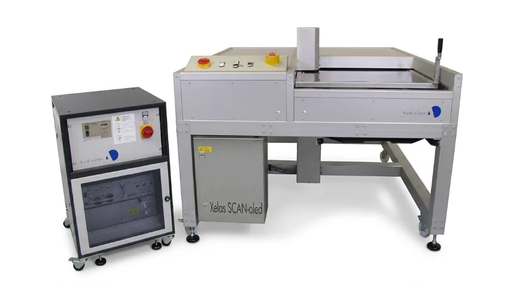
To meet diverse usage environments, the product line offers two configuration options: the Xelas LAB-oled system with a compact manual workstation for R&D; and the Xelas SCAN-oled option equipped with a mechanical sliding tray (up to 600x600mm) for higher measurement productivity. Thanks to the flexible software upgrade capability and the pre-established material database, the system can easily be expanded to address future challenges in measuring complex thin films.