
![youtube - [Video]](/web/image/product.image/547/image_128/youtube%20-%20%5BVideo%5D?unique=0ffae95)


Key features
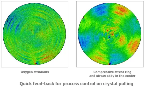
- Infrared scanning (SIRD Technology): Quantitative and accurate mapping of internal mechanical stress without causing damage or harm to the surface of the semiconductor wafer.
- Ultra high sensitivity (High Sensitivity): Detection of microstructural defects, subsurface cracks, and slip lines hidden deep beneath the surface of the wafer.
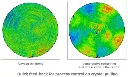
- Comprehensive mapping (Full-surface Mapping): Provides high-resolution visual images of stress distribution across the entire wafer from small sizes up to 300 mm.
- Optimal measurement speed (Fast Inline Scanning): Fast processing time, perfectly suited for both in-depth analysis in R&D and automated quality control on the production line.
- Diverse material compatibility (Multi-material Support): Effective measurement on various important semiconductor material substrates such as Silicon, SiC, GaAs, InP, and thin films.
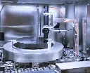
- Flexible integrated design (Automation Ready): Easily integrates with automated wafer handling systems (EFEM) and transfer robots in standard cleanroom environments.
Detailed description
Technology & Operating Principles
SIRD applies the birefringence effect due to stress. When polarized infrared laser passes through the wafer, mechanical stress or crystal defects will change the polarization state of the light. The optical sensor captures this depolarization to accurately calculate the amplitude, stress direction, and create a visualized digital map.
Intrinsic stress from cutting, grinding, or heat treatment processes is often invisible but causes wafer breakage and circuit faults in later stages. SIRD addresses this by using non-contact, non-destructive testing, helping to detect subsurface cracks and localized residual stress early. From there, engineers can easily optimize processes (annealing, thinning) and minimize waste.
Integration & Expansion
Equipment supports wafers from 100 to 300 mm, with flexible configurations from standalone machines for R&D to fully integrated automated handling systems (EFEM) for manufacturing plants. The accompanying software supports SECS/GEM connectivity, automatically identifies faults, and generates reports, meeting strict semiconductor industry automation standards.