


Key Features
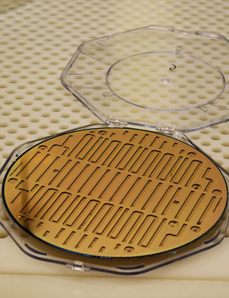
Optimized for large semiconductor wafers (6" & 8" Wafer Capability): Designed with precision mechanics to perfectly handle large 6 inch and 8 inch industrial standard wafers.
Superior in-situ alignment (In-situ Alignment 1 µm): The direct optical alignment system within the bonding chamber completely eliminates mechanical misalignment caused by wafer movement between processes.
Robust high force handling (High Force up to 40 kN): The motorized Z-axis applies uniform pressure over the large surface area of the 8" wafer, meeting the stringent requirements of diffusion or eutectic welding processes.
High power independent heating (Independent Heating): Separate temperature control for the upper and lower heating plates (temperature delta difference of up to 350°C), allowing for different heating rates to optimize the degassing process.
Wafer edge clamping to protect the surface (Wafer Edge Clamping): The clamping mechanism holds the wafer at the outer edge, ensuring no contact with the active area, minimizing the risk of contamination or scratching.
Support for complex multi-stack structures (Multi-stack/Triple-stack Bonding): Capable of performing three-layer welding (such as Si-Glass-Si) and stacked structures up to 30 mm thick while ensuring pressure uniformity.
Detailed description
Technology & Operating Principle
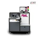
AWB 08 operates based on AML's proprietary technology platform, allowing for a closed-loop process: In-situ Alignment, Outgassing, Surface Treatment, and Bonding all within a single processing chamber. Throughout the process, the Live View camera system (or optional NIR for Silicon materials) enables real-time monitoring. The device integrates high-tech modules such as Radical Activation (RAD) and Automatic Vapor Chemical Spraying (AVI) to clean and enhance surface bond energy just before the two wafers come into contact.
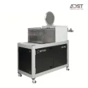
When transitioning from the R&D stage (typically using 3" or 4" wafers) to the pilot production or industrial production stage (requiring 6" or 8" wafers), engineers often face significant challenges regarding the uniformity of pressure and temperature over a large surface area, as well as the risk of film misalignment when moving wafers between the alignment machine and the standalone welding machine. AWB 08 thoroughly addresses this barrier by keeping the wafer fixed in a vacuum environment from the alignment stage until the welding is complete, while the 40 kN heating plate and mechanical axis system ensure extremely uniform force/heat distribution across the entire 8" wafer surface, minimizing product defect rates.
Integration & Expansion
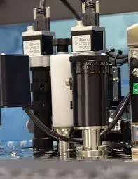
Although it does not support small chip clamp sizes (which is the privilege of the AWB 04 series), AWB 08 possesses strong industrial upgrade capabilities. The machine allows for the integration of up to 3 process gas lines, a high-power Turbo molecular vacuum pump system, fully automated alignment modules, UV light for adhesive curing, and a near-infrared optical system (NIR Optics) sensitive to wavelengths > 1.1 µm for aligning complex stacked microchip structures.