


Key Features
Superior in-situ alignment (In-situ Alignment 1 µm): The direct optical alignment system within the bonding chamber eliminates misalignment during wafer movement, ensuring absolute mechanical accuracy.
Powerful independent heating (Independent Heating): Allows for separate temperature control for the upper and lower heating plates with a difference of up to 350°C, optimizing the process for effective outgassing or getter film activation.
Extremely high mechanical pressing force (Up to 40 kN): Motorized Z-axis control allows for the application of a strong and uniform mechanical compression range for demanding bonding applications.
Safe wafer edge clamping (Wafer Edge Clamping): Completely secures the wafer by the outer edge, preventing contact with the functional surface, eliminating the risk of contamination or damage to the adhesive surface.
Optimized cleanroom footprint (Small footprint): A compact monolithic design minimizes the physical space occupied in a standard cleanroom environment.
Triple stack bonding capability (Triple Stack Bonding): Anodic welding technical support for complex structures such as silicon-glass-silicon and glass-silicon-glass with an overall thickness of stacked arrays up to 30 mm.
Detailed description
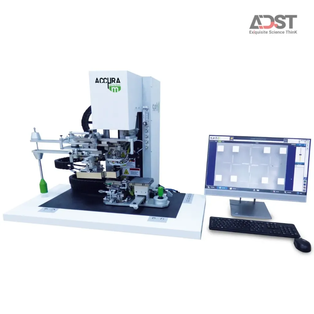
(1) Technology & Operating Principles
AWB 04 integrates the entire alignment and bonding process of semiconductor wafers into a single vacuum processing chamber. The device uses a direct optical alignment system (In-situ), allowing engineers to directly observe (Live View) the bonding surface and make precise adjustments before contact. The machine integrates advanced surface chemical processing technologies including Radical Activation (RAD) and Vapour Injection (AVI) to clean oxides (such as copper oxide) and enhance surface bond energy just before bonding.
Traditional wafer bonding systems typically require separate alignment (aligner) and bonding (bonder) equipment. Transporting aligned wafers from one machine to another can easily cause film misalignment due to vibrations, cleanroom dust contamination, and reduced outgassing performance. AWB 04 thoroughly addresses this issue with its "In-situ" mechanism — alignment, surface treatment, degassing, and bonding occur continuously on-site in a fully controlled environment, ensuring 1 µm accuracy and absolute cleanliness for sensitive MEMS or microchip components.
Integration & Expansion
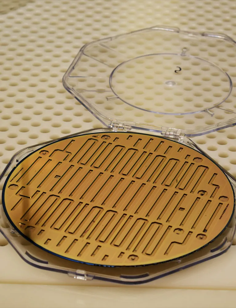
The device flexibly supports standard wafer sizes of 3", 4", and 6" along with the ability to customize the upper platen heating plate for bonding selected small chip sizes (10 mm, 15 mm, 25 mm). The system allows for flexible expansion: integration of up to 3 process gas lines, a UV curing system for adhesives, near-infrared optical systems (NIR Optics) for alignment through opaque materials like Silicon, or a fully automatic alignment module.