

Key features
- Smart counter-electrode: Applies pre-aligned routing design right from outside the vacuum chamber, eliminating the need for in-situ alignment, streamlining operation, and requiring no consumables.
- Superior spatial resolution: Provides 3D tomographic datasets approaching atomic level, allowing for the detection of individual atoms with excellent collection efficiency.
- Absolute analytical sensitivity: Provides uniform sensitivity for all chemical elements and their corresponding isotopes.
- Extended quantitative analysis: Performs accurate elemental concentration measurements over a range from sub-nanometer (sub-nm) to micrometer.
- Powerful 355 nm UV Laser system: The ultraviolet laser pulse module is designed to industrial standards with 100% automated beam focusing, flexibly expanding the research range from metals to semiconductors and ceramics.
Detailed description
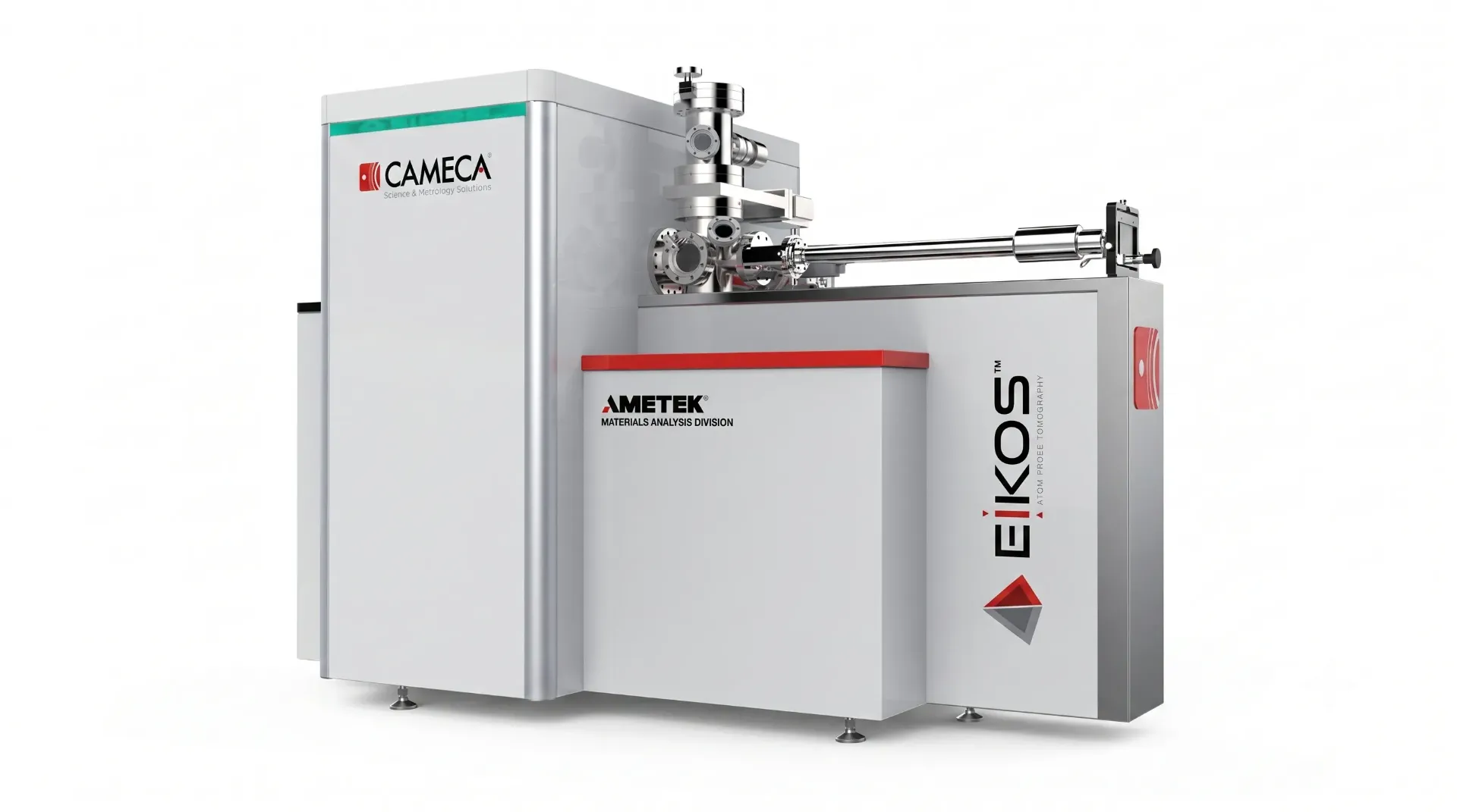
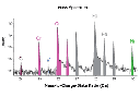
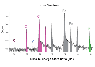
A new era of atom probe tomography (APT)
EIKOS-UV is CAMECA's groundbreaking material analysis system, inheriting 30 years of the company's success and designed to optimize both academic and industrial environments. The standard version (EIKOS™) operates in voltage mode combined with an electrostatic reflectron, providing extremely sharp mass resolution along with a perfect signal-to-noise ratio. In the full configuration version (EIKOS-UV™), the system is additionally equipped with a 355 nm laser pulse generator, allowing the device to easily separate complex material layers into an accurate 3D map regardless of the conductivity level of the sample.
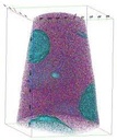
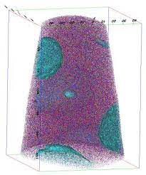
Unlocking microstructure & Grain boundary engineering
In the process of developing commercial alloys (Inconel, AlNiCo) or optimizing additive manufacturing materials, the separation of impurities at the grain boundary directly affects the mechanical strength and magnetic properties of the material. Quantitative observation of these phenomena at the nanometer scale is a significant barrier. EIKOS-UV completely breaks that "blind spot" with its ability to reconstruct 3D data, clearly indicating tiny impurity precipitates (such as aluminum and niobium nanoparticles) and sharply displaying the concentration contours across phases. Through this, engineers can easily understand how the thermal processing cycle affects the performance of superalloys.
Closed-loop analysis platform and automation
Aiming for ease of use, CAMECA provides a closed-loop process from sample preparation (with standardized kits for focused ion beam (FIB) milling and electrochemical polishing) to automated report generation. The "heart" of the system's software is the Atom Probe Control Center™ platform with an intuitive interface, combined with the specialized AP Suite and IVAS software. All ultra-large point cloud datasets are smoothly analyzed to instantly extract 1D mass spectra, 2D concentration profiles, or 3D spatial structures without requiring complex intermediate data processing.