Key features
Extremely high layer alignment accuracy (± 250 nm): Ensures absolute uniformity between complex micro-pattern layers during repeated engraving.
Ultra-fine structure resolution (Sub-50 nm resolution): Allows for the formation of ultra-small nano-sized details with perfect structural fidelity.
Optimal flatness and tilt angle control (< 1 µrad): Automatic Pitch & Roll angle alignment mechanism between the stamp and wafer base to ensure 100% even pressure distribution.
Outstanding cost-effectiveness (Cost-effective solution): Provides large area nano pattern production capability through the step-and-repeat method, minimizing the cost of manufacturing large monolithic molds.
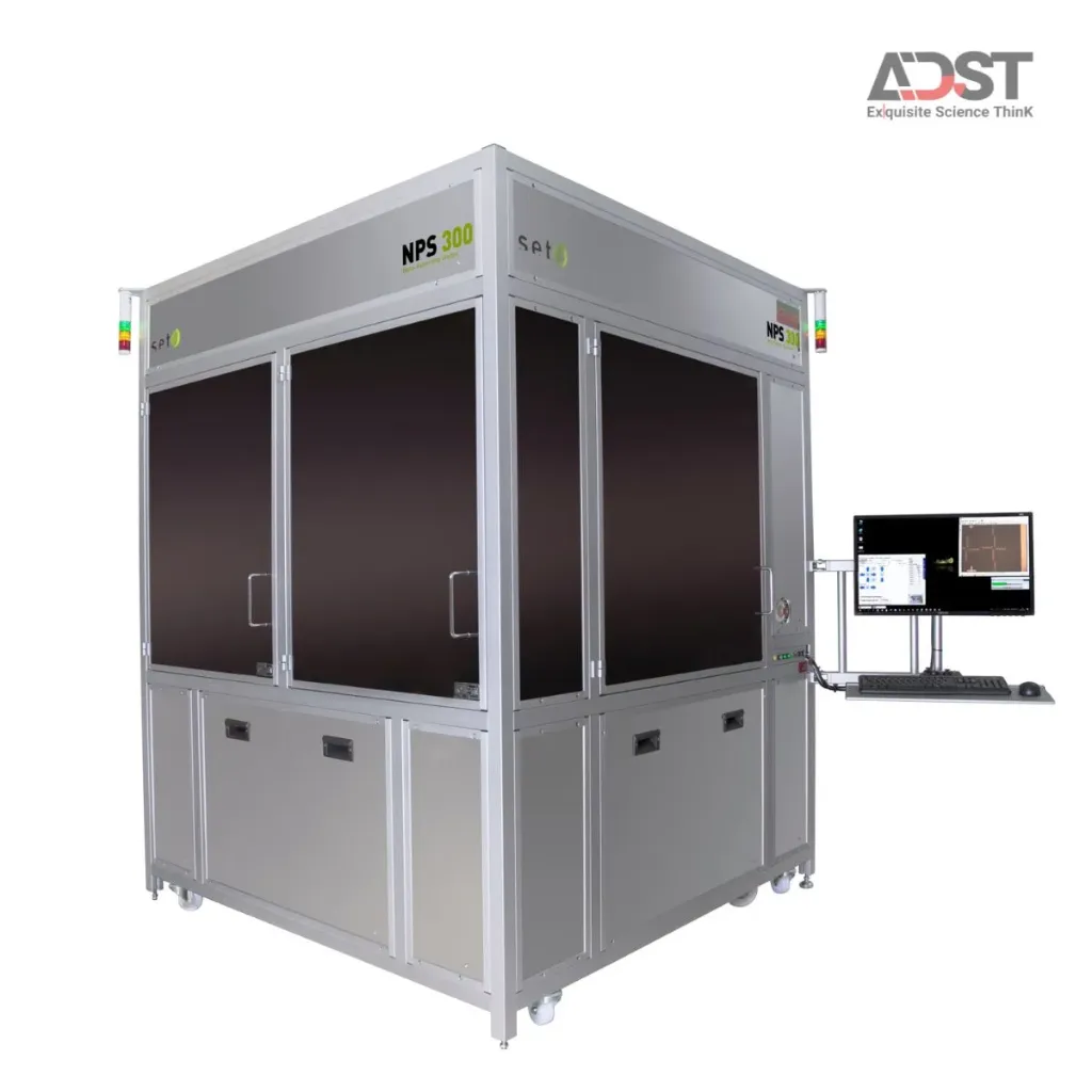
Compatibility with various substrate sizes: Supports flexible engraving processing on large wafers with diameters of up to 300 mm.
Flexible process conversion: Comprehensive support for both core engraving printing technologies, UV-NIL (using UV light) and Hot Embossing (heated hot stamping).
Detailed description
Technology & Operating Principle
NPS300 operates on the principle of nano imprint lithography using a stepper for repeated pattern stamping (Nanoimprint Lithography Stepper). The stamp carrying the nano structure will be precisely aligned by a high-precision optical system in contact with the photoresist layer on the substrate. Then, the system uses UV light energy (for the UV-NIL process) to cure the material at room temperature or uses high temperature combined with pressure (for the Hot Embossing process) to accurately replicate the structure from the stamp to the Wafer surface, then automatically moves to the next position.
The fabrication of nano structures on large diameter Wafer plates (such as 200 mm or 300 mm) using the full-wafer imprint method often encounters errors due to uncontrollable absolute flatness or the high cost of making large-sized stamps. The NPS300 completely addresses this issue with Stepper technology — breaking down the engraving process into multiple repeated cycles across each area. Combined with an automatic parallel alignment system under 1 µradian, the machine ensures even pressure distribution across all points, eliminating air bubbles and pattern distortion errors.
Integration & Expansion
The design platform of the NPS300 allows for flexible integration of technology modules according to research and production requirements. The system has the capability to handle wafer substrates from small sizes up to a maximum of 300 mm, integrates a standard wavelength UV light source, a curing temperature control system, an environmental isolation chamber, and allows for the expansion of the compression force range from very low levels for sensitive structures to high force levels for specific polymer/glass material embossing applications.