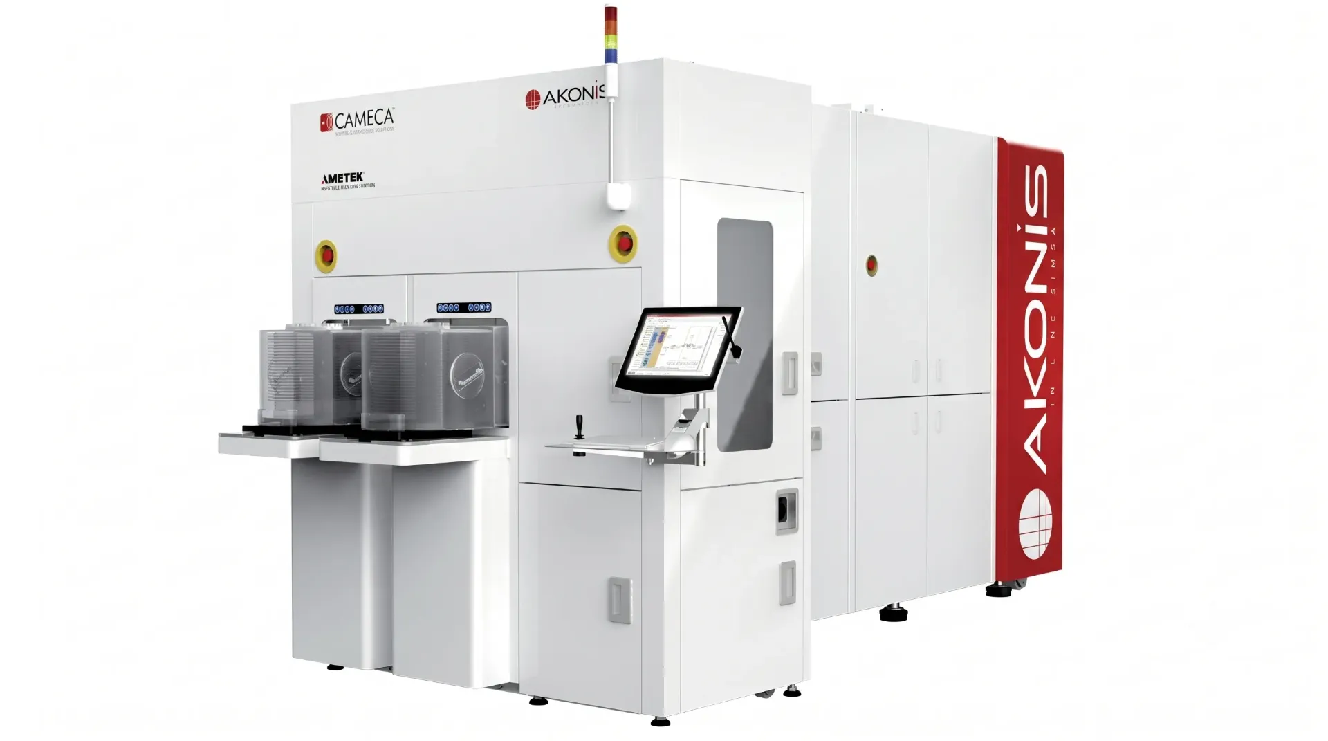


Key features
- High-density EXLIE column technology: Optimizes beam size (< 30 µm) and increases sputtering rate (> 5 nm/min at 150 eV), ensuring extremely high analytical throughput even on thick film structures.
- Comprehensive wafer surface measurement: Ability to inspect blanket and patterned samples directly on ultra-small 20 µm microchip pads thanks to the AI Cognex recognition system and ultra-precise interferometer sample stage (< 2 µm).
- Absolute automated operation: Automatically focuses the beam and adjusts secondary optics, combining near UV OCE charge compensation technology that allows technicians to operate the machine intuitively and quickly.
- Super-fast process response time: The loadlock chamber automatically loads samples in under 90 seconds, reducing over 97% of the wait time for feedback data to the factory line compared to traditional lab analysis processes.
- Low total cost of ownership (TCO): Integrates Brooks front-end wafer processing, durable Pfeiffer vacuum, and meets SEMI safety standards (S2/S8, E4, E5, E39, E84...), with a compact footprint design that fits sub-fab spaces.
Detailed description
Breakthrough In-line SIMS mass spectrometry technology
Building on over 60 years of CAMECA's leading experience in ion beam technology, AKONIS brings laboratory-level analytical power directly into the factory (Fab) line. The core of the system is the ultra-low energy ion beam technology EXLIE (< 150 eV). Unlike outdated SIMS systems, the high-density EXLIE beam combined with an optical architecture that collects extremely high resolution provides ultra-stable analytical signals and maintains maximum sensitivity without causing widespread damage to the chip surface.
Solving the HVM measurement and N5 technology node challenge
In the high-volume manufacturing (HVM) semiconductor production process, monitoring ion implant profiles and core material composition (such as SiGe/SiP chains) has always been a time challenge. AKONIS breaks this barrier with superior analysis speed of 8 wafers/hour. Notably, the advanced optical centering structure on the probe enables the system to achieve excellent repeatability and reproducibility (< 1%), becoming a key yield assistant for the advanced N5 CMOS process and beyond.
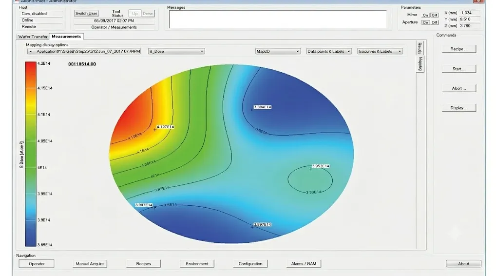
Intuitive software control platform
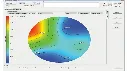
Completely eliminating the stereotype that SIMS machines are extremely complex academic devices, AKONIS is equipped with control software featuring a minimalist interface personalized for factory operators. The recipe configuration process is fully automated based on a proprietary material database. Engineers can flexibly generate quantitative reports and view detailed 3D graphical images of the mass spectrum, ensuring timely quality control according to the strictest processes.