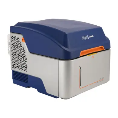


Key features
- High-performance SE & BSE detector equipped for imaging surface topography, high resolution (< 8nm).
- EDS point analysis, line scan, and full elemental mapping.
- Operates in both high and low vacuum modes, minimizing or eliminating charging effects on non-conductive samples.
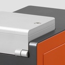
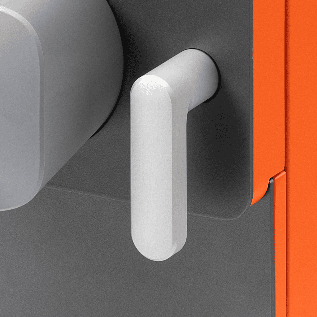
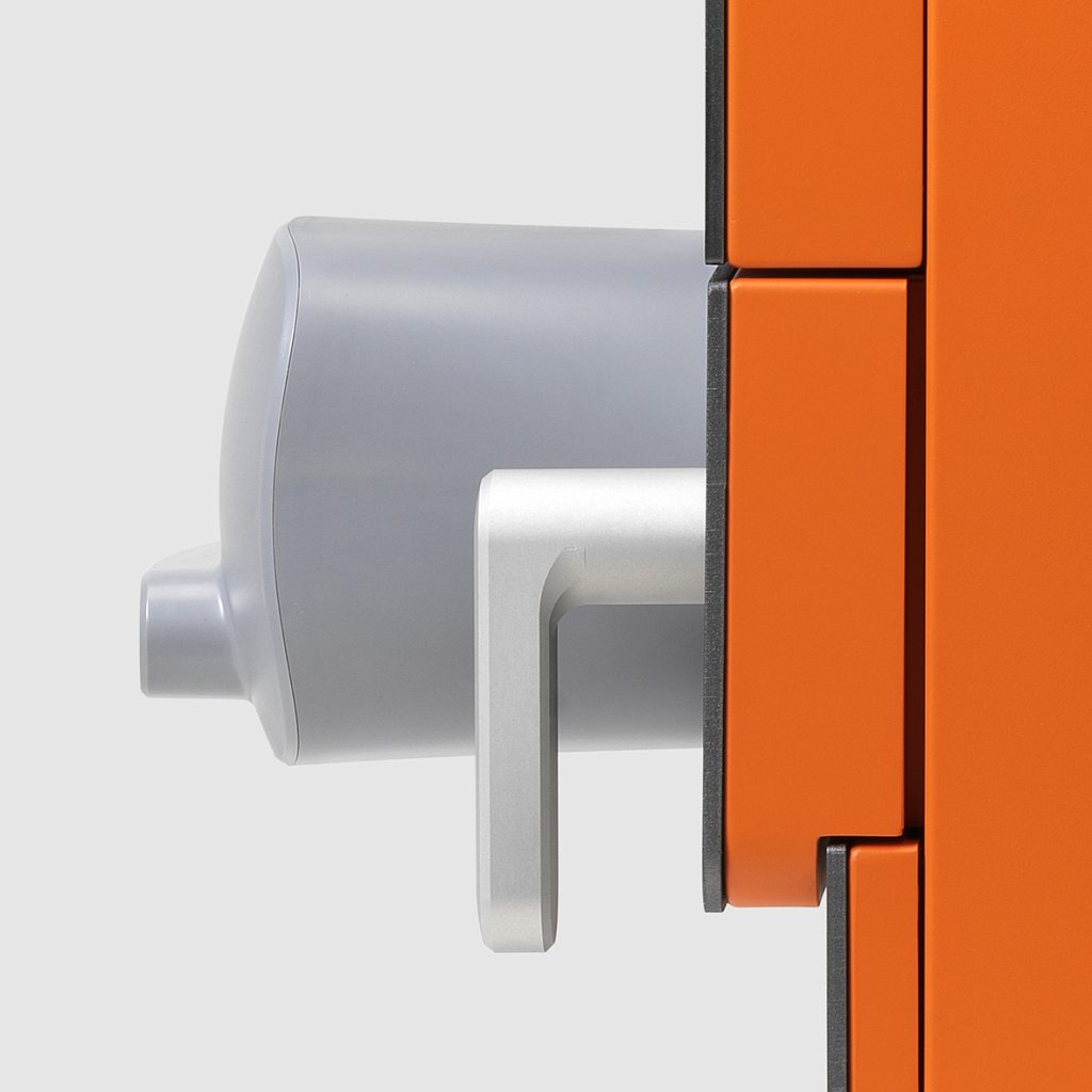
- Eucentric tilt stage ensures the specimen remains in focus when tilted.
- Electron source can be user-replaced with a simple alignment tool — no technician or specialist needed for inspection.
Detailed description
Technology & Principles:
NANOS is equipped with a Secondary Electron Detector (SED) and a Backscattered Electron Detector (BSD). The SED collects electrons emitted from the surface of the sample, creating sharp, high-resolution images that clearly show surface structure. The BSD, a high-quality 4-quadrant detector, provides compositional contrast by detecting backscattered electrons sensitive to atomic number differences. This design allows for enhanced imaging modes such as topographic shading.
Vacuum chamber and vacuum mode:
The clean vacuum chamber helps eliminate the risk of contamination and mechanical failure, ensuring stable imaging performance over time.
Two modes: high vacuum and low vacuum. In high-vacuum mode, non-conductive samples may experience charging effects, where electrons accumulate on the surface, causing image distortion. To mitigate this, NANOS is equipped with a low-vacuum mode that helps reduce or eliminate the effects of charging phenomena.
Switching between these two modes is very simple, with just a single click, allowing users to effectively manage different sample types and conditions.
Eucentric Stage - Standard Feature:
The eucentric stage ensures that samples maintain focus while tilted, without needing to adjust SEM settings. XY motion is controlled through software, while tilt angles are manually adjusted with real-time feedback on the screen. With a tilt angle of 55°, users can explore samples from various angles without affecting focus or image quality.
Economically optimized design:
Thoroughly addressing laboratory barriers with a high-performance filament configuration achieving over 1000 hours of lifespan, minimizing replacement frequency and significantly lowering technical service costs.
Integrated, expandable:
Semplor Discover EDS software: quickly establishing elemental maps to accurate identification and quantification. Streamlining every step in the analysis process delivers fast, reliable results without interruption.
- The Semplor Explore App transforms standard SEM image display into advanced material property analysis capabilities — particle, fiber, and 3D analysis ...