


Main features
- The “super tunnel” electron optical technology minimizes space charge effects, ensuring low voltage resolution performance.
- Electromagnetic & electrostatic compound lenses help reduce aberrations, significantly improving resolution at low voltages and allowing observation of magnetic samples.
- Ion beam column with a resolution of 3 nm @ 30 kV, with 72 hours of continuous uninterrupted operational stability.
- Nano-Manipulator installed inside the chamber, step size ≤ 10 nm and maximum movement speed of 2 mm/s
- Multi-aperture conversion system that automatically switches between apertures without mechanical movement, allowing quick switching between different imaging modes.
Detailed description
Principle & Technology:
CIQTEK DB550 is a system that operates based on the combination of a field emission scanning electron microscope and a Gallium ion beam converging column. The technology focus is the optical system SuperTunnel with an electron pathway that has no crossover points, combined with a mixed electric-magnetic field lens cooled by water for thermal stability, helping to minimize optical aberrations and optimize beam density.
Stable Ga⁺ ion beam and the Specimen Exchange Loadlock sample locking system
In advanced semiconductor chip research, preparing standard thin samples for transmission electron microscopy is extremely difficult due to the samples being easily structurally damaged or contaminated, magnetically contaminated, and locally charged under the beam. CIQTEK DB550 thoroughly addresses this issue thanks to the stable Ga⁺ ion beam and the Specimen Exchange Loadlock system compatible with 8 inches.
Mixed electric and electrostatic objective lens
The non-magnetic compound lens allows for the processing and analysis of cross-sections for both magnetic and non-conductive materials without distorting the image. Combined with the Scanning Transmission Electron Microscopy (STEM) optional probe, the device allows for imaging bright field (STEM-BF) and dark field (STEM-DF) of microchip device layers to perform Failure Analysis accurately.
Integration, expansion
- Integrated system with a nano manipulator controller with a step size of ≤ 10nm.
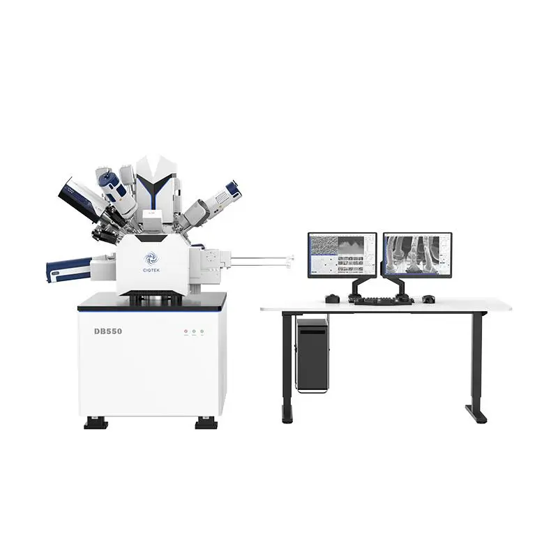
- The photo capture and image processing functions are integrated into a general user interface, with reference comparison images displayed on the left and right.