
![youtube - [Video]](/web/image/product.image/535/image_128/youtube%20-%20%5BVideo%5D?unique=eeb8d60)

Key features
Accuracy ±0.5 µm: Ensures ultra-precise alignment for advanced microelectronic and optoelectronic components.
High flexibility: Optimized for various applications, allowing easy configuration changes and testing parameters.
User-friendly, accessible design: Simplifies operation and maintenance processes, enabling users to quickly master the equipment.
Cost-effective investment: Delivers the performance of high-end industrial machines at a budget-friendly price for R&D.
Optimized for universities and research institutes: Perfectly suited for intensive research environments, prototyping, and small-scale production.
Detailed description
Technology & Operating Principles
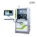
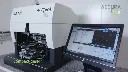
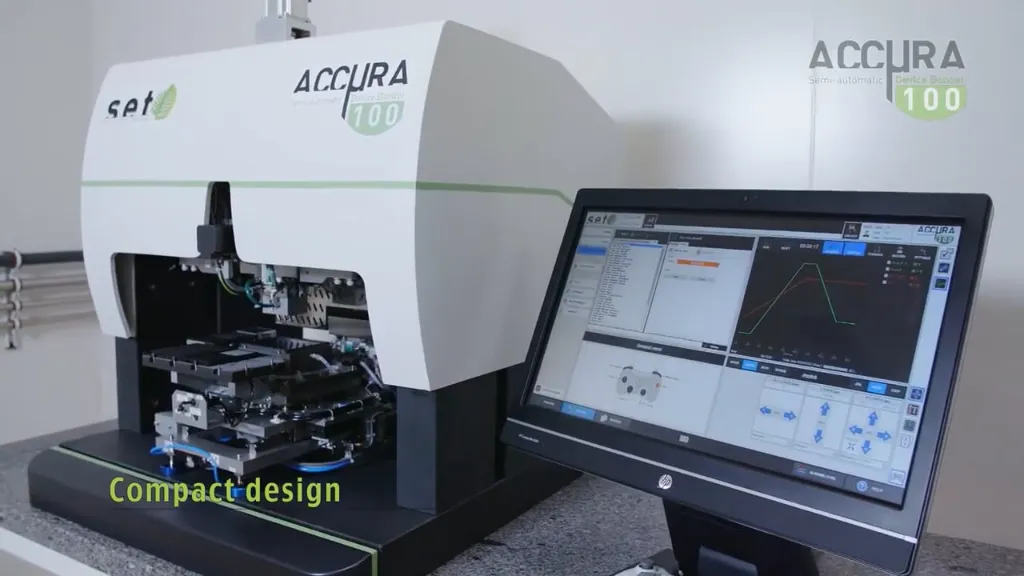
The ACCµRA100 is a flip chip bonder that uses high-resolution optical alignment technology and a digital force/temperature control system. The machine presses the chip surfaces containing bumps directly onto the substrate with extremely high mechanical precision, achieving an error margin of ±0.5 µm.
Research institutes and labs often face difficulties when choosing between: a low-cost manual soldering machine with poor accuracy, or a high-precision industrial machine that is expensive and overly complex to operate. The ACCµRA100 completely addresses this issue. The machine provides optimal accuracy of industrial equipment but features an intuitive, accessible interface and a very reasonable price for R&D budgets.
Integration & Expansion
The device has a flexible structure, allowing users to easily upgrade or integrate additional functional modules according to research needs such as: thermo-compression, ultrasonic soldering, or conductive adhesives (ACA/ICA). The machine is well compatible with various chip sizes and substrate materials, from optoelectronic components to micro-electromechanical systems (MEMS).